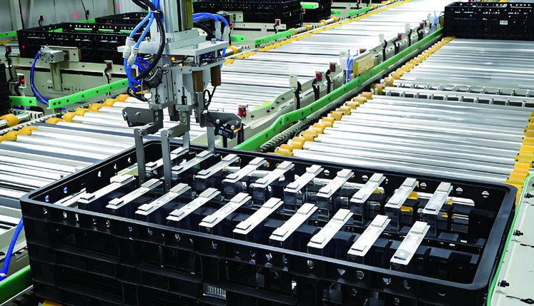
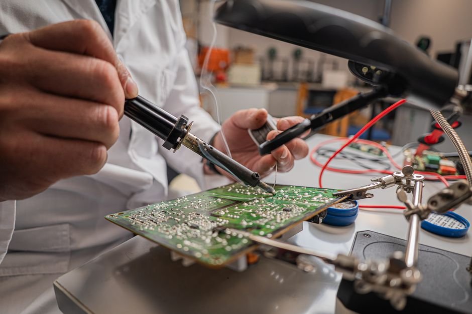
Silicon has a useful secret: it is opaque to the eye but transparent to short-wave infrared. Below the surface that visible-light inspection sees — past the polished top of a wafer, under the mold compound of a packaged die — SWIR imaging sees the interior: cracks, voids, delaminations, misaligned bonds. For anyone sorting, inspecting, or reclaiming silicon, that is the difference between judging a part by its skin and judging it by its structure.
This case looks at how a semiconductor packaging house built a SWIR inspection capability — for incoming wafers, bonded stacks, and reclaimed material.
Project Background
In 2024, the quality engineering team of an OSAT (outsourced assembly and test) facility in the Yangtze River Delta reviewed a painful quarter: two field returns traced to die cracks that had passed every in-house inspection, and a growing reclaimed-wafer program whose yields were unpredictable. Their inspection stack was the industry default — high-resolution visible microscopes for surface defects, X-ray for wire-bond voids on sample basis, electrical test at the end. Subsurface wafer cracks, edge chips hidden under tape, and die-attach delaminations sat in the gaps between those tools: visible light could not see them, and sampling X-ray was too slow for coverage. The reclaim program had a matching problem — sorted by surface appearance and electrical probe alone, lots of supposedly good reclaimed wafers carried hidden damage that only appeared as early-life failures downstream. The team funded a SWIR inspection station: an InGaAs-based 640×512 SWIR camera with through-silicon optics on a motorized stage.
Pain Points of the Traditional Approach
- Visible light stops at the surface. A crack propagating inside the wafer bulk, a void under the die, a delamination under mold compound — none of these disturb the surface a microscope sees until the part fails.
- X-ray coverage does not scale. X-ray inspection is slow and dose-managed; used on samples, it estimates a lot’s quality rather than guaranteeing each part’s.
- Electrical test is a lagging indicator. A part with a subsurface crack can pass every electrical test and still fail in the field when thermal cycling grows the crack — exactly the failures that cost the most.
- Reclaim sorting by appearance is a coin toss. Reclaimed wafers graded on surface and probe data carried hidden structural damage into production, turning a cost-saving program into a reliability risk.
The Thermal Imaging Solution
The station images wafers and packaged parts in the SWIR band, where silicon transmits: an InGaAs camera with illumination behind or beside the part makes the wafer’s interior visible as a live image. Subsurface cracks appear as dark lines against transmitted light; edge chips show through grinding tape; die-attach voids and delaminations read as shadowed regions under the die.
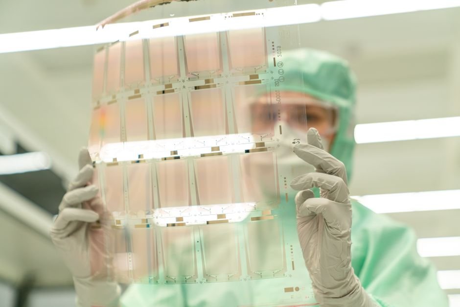
The workflow runs at inspection-line speed, not lab speed: full wafers are scanned on the stage in seconds per field, with software flagging suspect regions for operator review. The reclaim program put the same station at its intake: every reclaimed wafer is now imaged through its thickness and sorted by its actual internal condition — good material goes to production, marginal material to low-grade uses, damaged material out — instead of being graded by its surface.
What the Thermal Solution Changed
- Subsurface defects became catchable. In its first quarter, the station intercepted die cracks and die-attach voids on parts that had passed visible inspection and electrical test — including the failure class behind the two field returns, which has not recurred.
- Coverage replaced sampling. Through-silicon imaging at stage speed made 100 % inspection of critical lots practical; X-ray sampling is now reserved for the cases it uniquely answers.
- Reclaim yield stabilized. Sorting by internal condition instead of surface appearance cut the reclaimed program’s downstream failure rate by over two-thirds, turning it from a reliability risk back into a cost saver.
- Root causes got photographs. Process engineers now see the defect — where a crack nucleated, how a delamination spreads — which has fed back into dicing and bonding process changes, not just sorting.
Module Selection Notes
Through-silicon inspection needs a SWIR camera with good quantum efficiency across the silicon transmission window, low read noise for clean transmitted-light images, and optics matched to the stage. The SPECTRA S06A SWIR module (InGaAs, 640×512) is built for exactly this duty; where heat signatures matter alongside structure, pair it with a thermal core such as the SPECTRA L06A 640×512 LWIR core. See the scientific research application page for lab and inspection patterns.
Building a wafer inspection or material sorting station? Talk to our engineers about SWIR core selection, illumination, and stage integration.